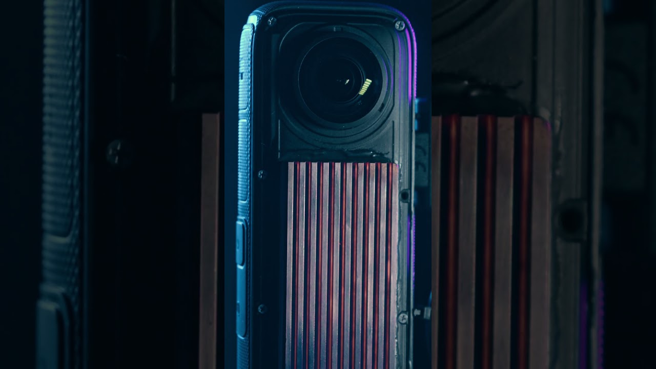
Speedrunning 30yrs of lithography technology
Machine-readable: Markdown · JSON API · Site index
Machine-readable: Markdown · JSON API · Site index
Экстракты и дистилляты из лучших YouTube-каналов — сразу после публикации.
ПодписатьсяЛучшие методички за неделю — каждый понедельник