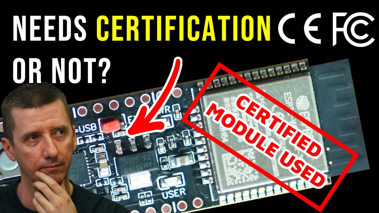
From estimated 10 weeks down to 1 week. Real examples showing how AI helps with component placement and PCB layout. Thanks to Sergiy Nesterenko and Ben Jordan from Quilter.
Links:
- Quilter: https://www.quilter.ai
- Sergiy's LinkedIn: https://www.linkedin.com/in/sergiynesterenko/
- Ben's LinkedIn: https://www.linkedin.com/in/benjordan-principle-ee/
- Project Speedrun technical write-up: https://www.quilter.ai/blog/preparing-an-ai-designed-computer
- Get started: https://app.quilter.ai
- Ask your questions about electronics here: https://fedevel.com/assistant
- Easy search through my videos: https://fedevel.com/hw-assistant
- Learn more about electronics, check out our online courses:
https://fedevel.com/courses
Chapters:
00:00 What is this video about
00:42 What makes Quilter different (focused only on layout)
02:09 Not an LLM, not ChatGPT: a geometry and physics problem
04:16 Inspired by DeepMind's AlphaGo and AlphaZero
08:57 Integrations: Altium, Cadence, Xpedition, KiCad
09:39 There is no magic button. Quilter is a tool, not magic
10:39 The Goldilocks zone: 200 to 1,000 components
14:05 Demo 1: a custom RP2350 microcontroller board in Altium
18:01 Uploading to the Quilter web app
32:52 Auto-detecting switching regulators and bypass caps from the schematic
44:48 Kicking off the placement job
52:35 Reviewing the first placement
53:57 Why floor planning is essential for high-quality results
1:32:16 Customer success criteria: "do I start from scratch, or start from Quilter?"
1:35:25 Demo 2: Project Speedrun, a full Linux-capable computer
1:37:49 Robert guesses how long the layout would take
1:40:07 The real quotes: 350 to 450 hours from professional contractors
1:41:13 Ben's one week of cleanup, fabricated at Sierra Circuits
1:44:33 Validation: Linux, Ethernet, USB, HDMI, Chrome, browser games, Doom
2:00:21 How to get started
2:02:06 About Quilter: 6 years, 35 people, $40M raised
------------------------------------------------------
(C) FEDEVEL by Robert Feranec
https://fedevel.com
Оглавление (21 сегментов)
What is this video about
In this video, we are going to talk about AI in hardware design and uh we are going to have a look at one of the companies Quilter and uh SI and Ben are going to explain uh how this is going to work, what to expect and maybe you know where AI could help us. Is this what we are going to talk about S Ben? — Yes sir, let's do it. Okay. So, uh there are number of AI companies or companies doing AI in hardware. Uh what is different in Quilterra or what is your main goal? — Yeah, let's dive into that. So, uh
What makes Quilter different (focused only on layout)
the first thing to state is at Quilter, we're explicitly focused on the layout portion of PCB design. Um so, we've taken a very strong stance to go specifically after layout. Um, and this comes just from my own personal experience working at SpaceX before starting the company, seeing that be a bottleneck. Uh, bottleneck for flight designs, bottleneck for test designs, bottlenecks for test automation, and for just for just about everything you could build. Um, so the kind of approach that we're taking is to really spend all of our resources and all of our time trying to make layout faster and to leave schematic to leave uh, you know, everything else kind of as is. Um, so we are not really helping people um, you know, uh, come up with schematic or find parts or even create footprints. More often than not, companies we work with have librarians. What we're really trying to do is get a layout from, you know, 3, four weeks down to a week or a couple of days. That's kind of our goal. Um, now the way we do that is we treat this uh, really as a kind of um, exploration problem, right? So we see that layout is something where you can propose a bunch of different variants or approaches to solve a board. There is sort of a way to compute whether or not the board uh should work or not, right? Like does it meet signal integrity requirements, power integrity requirements, DFM requirements, so on and so forth. And ideally you have an algorithm that can propose variance of layouts until it meets all the constraints necessary for it to work. Right? That's kind of where we're going.
Not an LLM, not ChatGPT: a geometry and physics problem
And so one kind of obvious thing uh just to state real quick is um this is not an approach where we're using LLMs or OpenAI or anything like that, right? We don't view this as a language problem. We geometry and physics problem. So we're developing all of our own models, all our own computational geometry engines, optimization routines to deal with the geometry and not relying on you know chat GPT or anthropic or whatever else. — Oh, that's cool. So uh before we continue, I would like to point out actually we will also do uh some demo. So everyone who is watching you will see what are the steps of doing layout with your system and uh then we will also have a look first we will have a look on this simple board and then we will explain how this can be used and how it was used for more complex board. uh I would like to point out so you mentioned you are actually building your own model correct — correct — and uh I think many people they would be worried because I've seen it also all over the internet I had same worries like where do you get the data yeah this is a really good question so the answer is we don't fundamentally right so there is a data piece to this but it's worth explaining how it comes in exactly so the typical use case for how to build an AI model and in particular an LLM since that's the dominant case um the way that LLMs are trained today kind of very naively ignoring a lot of the more recent developments is this process called supervised learning basic idea is you take a Wikipedia page or a Reddit forum you feed in the first paragraph somebody says and you train the model to reproduce what the next person would have said and if you do that over all of the text of the internet you get you know the basic versions of chatgpt right That's an example of supervised learning. That's only one way to train a model, right? And it's useful when you want to mimic human behavior. But what we want to do is not necessarily mimic human behavior. solve the computational geometry, thermal and electromagnetic problem of a layout. That's different, right? We don't necessarily need to mimic a human for that. So the approach we take is
Inspired by DeepMind's AlphaGo and AlphaZero
heavily inspired by what was done by Deep Mind in 2017 when they created AlphaGo and Alpha Zero. Um so for those who aren't familiar, DeepMind is a research group in the UK that uh you did a lot of the early work in um neural networks and training. uh and their most famous or one of their most famous results was that they were able to beat a uh champion of the world in the game of go kind of like a game like chess for those who don't know go and uh the approach they took is one of reinforcement learning where basically they had their model play the game against itself and whenever it won it would make the moves that it took more likely and whenever it lost it would make those moves less likely. And after you do that billions and billions of times, the model on its own learns how to get really, really good at go without necessarily a human example. Now, there's more history here, but at the end of the day, that's how the best version of that system worked. — So, our approach is kind of similar, right? We are not recording a bunch of electrical engineers and watching exactly how they route, right? Like Ben has not created a data set of two billion boards for us uh that we have like recreated. as much as that would be fantastic. Um we just don't have enough Benz for that to happen. Um so what we have to do instead is we have people like Ben teach us about what are all of the rules, right? Like what are all the DFM rules? DRC rules? But even more importantly, what are all the important considerations like hey I have bypass capacitors, I have switching converters, I have return loops, I have um cross talk considerations, so on and so forth. And how do we approximate and compute them, right? and know whether or not we've succeeded or failed at that concern. That gives us the score and then the model can sort of start out at first playing randomly and then eventually get better and better at this. Now, that's the of course the naive explanation of how this works. In reality, there's a lot more to it than that. Um, if you look at the backgrounds of our team, a lot of us are from backgrounds of like computational geometry, 3D metal printing, uh, self-driving cars, and there's a lot of just actual classic algorithms and code that go into this as well to make the problem tractable, right? Um, but overall, the philosophy of the company is that whether or not a board design is good is a computable question. And if it's computable, you can have an algorithm attempt many, many, many times to solve it. and eventually gets better and better at meeting all those constraints over time. Mhm. I would like to highlight this because uh I think many people they think uh this AI in hardware design is hard to do or it's uh impossible to do because there is not enough uh boards available on internet and not only not enough boards but not enough good boards — to kind of use for the training. So that's not the way what you are doing. You are actually teaching your system based on physics and rules and system teaches itself automatically what is good what is bad and it will figure out the ways to do it properly maybe even different way than human are doing this but it may be at the end it may be even better layout correct — it's possible I mean I think that people are right that it's hard let's start there right like let's not overpromise promise out of the gate. This is very hard. We have a long way to go to truly master this. This is not something where, you know, you can just install a Python package called reinforcement learning, give it keycad or something in ANCIS and say go. Like if that was the case, this company would have existed a long time ago. Um the reality is even with modern reinforcement learning, even with modern simulation tools, even with modern CAD engines, all of that, it's still really, really, really hard. — But the philosophy of the approach I think makes sense, right? the velocity approach is something that has the potential to eventually make better boards uh than we have really time to make as humans, right? Because it's so laborious. Um but we're not there yet. For now, let's just focus on how do we get you from a two or three week layout to one week, right? That would be a win for all of the customers that we currently deal with. — So this is very important again to point out. Uh, so if someone is expecting one big button like do my layout, that's not what we should be expecting. Correct. — No, absolutely not. Yeah. The reality is that uh at the end of the day like it's a tool, right? Like and we and you'll see throughout uh as we talk about how we've built the system, we've very much baked in the concept of treating it like a junior engineer, right? So very purposefully we've left a lot of your control as an electrical engineer in the tools you already know
Integrations: Altium, Cadence, Xpedition, KiCad
right so we very directly integrate with Altium in this case uh but also with cadence also with expedition also with keycad for the hobbyists um we all of the iteration that we do with these boards and iteration's important um you still do in your CAD tool that you already know and the way to really think about quilter at this point is like you have an intern or junior engineer who's new at your company and you've given them a simple board and every couple of hours you stand over their monitor and say, "Oh, no, don't do this. Do that. Rotate this. Change this. " And with that, you know, you get in a few five minute check-ins, you get to a layout rather than doing it all yourself, right? Like that's the better model for how we can operate today.
There is no magic button. Quilter is a tool, not magic
— Mhm. — There's definitely no magic button. I would like to again point out when we are talking about small boards small I mean like let's say 10 20 50 components on the board this may not be so visible but if we are going to boards with hundreds or thousands of components and thousands of nets and vas and everything this can be actually very uh big timesaver correct that's why you are doing this because I think many people they don't realize When uh you have, I don't know, board with 3,000 components, you have to go and pick every single component, maybe move it to correct position, double check, then go pick another one. And if it takes like 20 seconds to handle one component, if you have 3,00 you can multiply it, and then you have to connect every path. If the component has at least two parts, it's going to take a lot of time. So this is where you would like to save the time initially. Correct. — That's correct. So when we um you know
The Goldilocks zone: 200 to 1,000 components
when we have customers coming in asking about the product, asking about where to try it out, um we steer them into what we call the Goldilock zone for Quilter, right? And in a lot of cases, if your board is like uh just a simple interposer board with two connectors and something like that, uh we're not going to be particularly helpful, right? Like you could probably knock it out in an hour or two yourself. By the time you learn how to use Quilter, it'll take as much time, if not more. It doesn't make as much sense yet, right? as our quality and polish increases, maybe that use case will make sense, but that's not where the focus is today. Um, conversely, if you go for boards that are way too big, right? Like if you give us a data center card or a full GPU, um, it's just so much that we just can't handle it, right? So, we can't help you there either. — But sort of between like 200 components to a,000 components is this really nice sweet spot where — probably the bulk of designs in professional companies are in that sweet spot anyway. um especially when I think about test boards and engineering samples and you know early exploration cards and things like that um and those are taking 2 3 4 weeks and we can pretty reliably compress that down to a few days right with exactly the method you're talking about of like eliminating a lot of the laborious parts uh still giving you the control but expecting some cleanup and some oversight. Um so the board we're going to show it first is not the main use case, right? like um certainly we have people who build boards like this and um we do have a free version of the platform up for kind of hobbyists and people who just want to poke around. You're welcome to it. Hundreds of these are being made every day on that. That's great. But like we're really focused on the ones that a professional is spending two three four weeks doing uh you know at a at an aerospace defense company or automotive company or at a consumer goods company or something like that. — Mhm. Okay. So in this uh kind of demo we are going to have a look on simple board just to show the steps to explain that everyone understand uh how this more complex board are going to be designed what steps need to be used and we are going to use this uh Raspberry P microcontroller and I think Ben is going to do this kind of work correct — right yeah so we start with something small just because it takes a lot less time to walk through the steps. Um, and I just wanted to add to something Sergi was saying there too, like e even if I wouldn't throw a, you know, 5,000 10,000 component design into quiltered today, um, designs like that tend to be like very large designs already tend to be, uh, somewhat partitioned. So, you know, that's another use case that we're seeing is some companies that have to do very big difficult things um can actually divide them up into smaller pieces and treat them as separate designs and run them in parallel. That's the beauty of this kind of system is um because it's software as a service basically. It runs in a server and I can upload to it and I can have as many jobs running in parallel as I want and that's actually super helpful and I've adopted that as a part of my integral part of my workflow. So I will start with a design like this. — Okay, I'm curious. Um, and obviously, yes, this is kind of a simple, it's just a microcontroller board with an RP 2350.
Demo 1: a custom RP2350 microcontroller board in Altium
And you'll notice that I'm using um in Altium what's called blankets. We'll come back to that in a moment. Um, but at the simplest level, just to poke this with a stick. Um, you'll see I've got, you know, everything's on one sheet. It's pretty simple, but I could have a multi-heet. It we it could be hierarchical. It doesn't matter. All right, that's all supported. And I've got my bypass caps directly connected to VCC pins up here. Um, I've got my USBC U type-C USB 2 connector there. Um, that's reversible IO. There's a the crystal oscillator down here. Um the RP 2350s are wonderful in that they actually integrated this switching actually I think the earlier version had a switching regulator integrated as well if I recall. Maybe it was linear, I don't remember. But um so we've got this switching regulator here. We've got another one up here for um stepping down the um USB input. could go anywhere up to 20 volts if it's USBC. So that's regulated down to 3. 3 for the system. Um, and so I've got a fairly welllaid out schematic. I've got a differential pair defined for USB 2. Um, and then this is the normal starting point, right? The — we very much it's human with AI. Human in the loop, AI in the loop. how whichever angle you want to do it, but I will always start with um basically my board outline and any critically placed components. — All of this is pre-done on my side. Um — so you did this, you imported the schematic into PCB, you draw the basic shape and place the critical connectors or the connectors where — the connectors where we know the places. — Exactly. and the push buttons. Um, if I wanted if I had any specific positions for LEDs or any sort of user interface or anything that's mechanically required to be where it is. — And here's the cool thing which we'll come back to later as well is that any copper I put on the board um for pre-outing anything is also left alone. Quilter will keep it as it is. anything inside that PCB boundary, it treats that as sacred and it won't tear it up or modify it. So, so it also allows for me to adopt my reuse practices as well, which is very much sort of leveraging um that side of things as well. Again, if I petition a design up and even if I'm using Quilter to do a certain chunk of something, if I work with Quilter and um get the routing and placement really good for an IC and its surrounding components, then there's nothing stopping me turning that into a reuse block and reusing that over and over again. And Quilter doesn't have to compute that every time. So, you know, it's going to also accelerate the process for things that are pretty common. — But I'm sorry for interrupting, but I would like to uh point out it's really cool. It uh doesn't touch the things which are already there because — it's you know when I was trying AI and I asked to write some software, you never know what it will rewrite. So I really don't want to have this kind of PCB where I run it through AI and it will randomly change something what I already checked or I'm happy with. — Yeah. So exactly. Yeah. So um in my
Uploading to the Quilter web app
browser here I've got Quilter already running and I already have in just to save time with the demo I already have this project. But normally the workflow is I'll create a project. I'll give it a name. I'll just call this one RP 2350. — Um U B I'll just call that's an A actually uh RP 2350A. So I have this new project and then it's like ready to accept files. So again, Sergi already mentioned we support Allegro, Expedition, Altium very well. Um, and Keycad as well of course and before you saw from Alteium I just explored the project directory. I have a lot of stuff here as well previously open just to accelerate the demo process. But normally we would take the project file uh that is not the correct I don't know why I've got that there. Somehow I duplicated that with a double dot. This is the correct one. And then I have the schematic. — Mhm. — And the first board which has no rooms. I didn't synchronize the rooms from schematic to PCB. I just want to show you don't have to use rooms. Um and a board like this probably most people wouldn't bother because it's so small and simple. And then we're uploading that. It's uh it's parsing the files. It's detecting all the information that would be needed. Now in the past even here in the past with some auto routers uh of yesterday year and one of the reasons people hated using them and didn't believe they will ever amount to much is cuz all they did was actually the board routing. You still had to place the components. set up all your DRC's. Now, don't get me wrong, again, it's not a big red go button. You are in charge of your design and ultimately you are responsible for its release. And so there is some setup involved, but with part of this reinforcement learning framework, we're able to parse and interpret and intelligently present a lot of the issues with design that lead to design rules and so on. And so all of that information — Yeah, I have question. I am going to interrupt. Sorry. — So first uh make it clear. So if someone would like to try it or use uh your system they go on your website uh of course they need to have account and I guess uh is it like publicly available now or they have to — it is yeah what I'm doing today is released in the public and anyone can sign up for an account to evaluate it. — Yeah. So do you wanted to say something there? — Yeah I'll just say it's probably relevant for your audience in particular. Um, you know, if you just go to quiltered. ai, you can log in, sign up, there's no restrictions. Go for it. Um, that's kind of our free version. Uh, and our free version is not meant for commercial use. Um, you know, that data, uh, we do, um, you know, speaking to the kind of training and whatnot, um, we do take the boards that you give us on the free version and then we slice them up into new boards, new problems that we give ourselves to solve. Right now, for commercial customers, that's not acceptable. So for commercial customers, they'll have uh they'll reach out to us, schedule a demo, uh and then we'll set up a commercial account where that doesn't happen. And with the more serious kind of aerospace and IP sensitive customers, we can even deploy this on premises. — So we can — Yeah, very important. Uh right, I mean especially here in the US, um you know, our defense industry is in a very important part of this puzzle. uh and you know with things like it and uh and kooi and ear and whatnot um yeah the only really way to do it is to give it to you on premises put it behind your aircraft servers uh let you control the full installation and no access to the internet needed no call to chatpt needed it's just a piece of software from that perspective um so if you're one of those folks you know come schedule a demo and we'll help you get set up with a pilot that's suitable for that uh but if you have just a open source design or some non-commercial design you want to play with yeah come upload throw it in have fun — and it's free. Yeah. If you are doing this free or open source board, you don't have to pay. — Correct. — Okay. And then so they go on your website uh they will upload the project exactly as Ben uh showed. Now uh first questions what first question what I had I know some answers because we had already called before but I would like to clear this uh what about the rules and stab and this kind of stuff because you know uh how does it know what it can do now? Yeah, that's a good point. And I didn't actually highlight any of that, but I did have a basic set of design rules already configured in Alteium. — Oh, the board. And that is also parsed and understood. Um there are certain rules that uh that we're not handling at all today just because they're nothing to do with route placement and routing. But all of the things like clearance, widths, um uh it knows what out what the differential pairs are. Um all that critical stuff for routing the board correctly and placing the parts has actually been posted and interpreted. But I have a chance also to review that and make some adjustments as I go. So we get a preview. You can see that that's there and that's actually what you're asking about is the very next step. So first it's brought in and it's showing me for confirmation. This is the layer stack that's defined in the board as I had already defined it. — So I have it's a four layer board. I've got top and bottom for routing and two inner ground planes for it you know good signal integrity. If I wanted to, if I renamed this, even in Alteium layer stack manager, if I named this L3 power or PWR or something, um, Quilter would understand it was intended to be used for power planes and, um, it would, in that case, I'm maybe jumping ahead a little bit, it would pick the most commonly connected power net in my design which in this case would be 3. 3V is the net name and it would give me one big uh power plane on that layer for that net. — So like you have a lot of control on the input and what you give it now right now that's what it's obtained from my board. If I wanted to, there's a basic library of different um you know existing what we call compile targets — um from different manufacturers or uh fabrication aggregators with different basic clearance rules. But 99% of the time what we found is people already have a layer stack in mind and they want us to target that. So that's what we're doing here. And I've reviewed that and I'm satisfied that has all been read in correctly. And next thing from my Altium design rules, it's also passed those and found the minimum fabrication required constraints that I've put in there. So in in my design, the fab I'm targeting happily goes down to 4 mil trace and space. So that's my minimum track with minimum clearance. Um and my preferred and minimum via uh design in Alteium Alteium's design rules uh is where you define VAS in other tools. It's in a pad stack. Um but it get it's got that information too. So I'm using 16 mil VAS with 8 mil holes or drills — and a 10 mil board outline margin for copper and traces and so on. Then the only other thing I would add here is I'm probably going to choose what's my desired component to component clearance. — Now on a board like this, I'm a bit under 10% u placement density for the board outline shape and the number of parts in their rough area. It's estimated uh and it showed this on the previous summary page after import um that I'm at about 10% routing or 10% placement density. So in this case I would say I go for I could go way less for component placement clearance. I could go down to 10 ms easily. um the fabricator and assembly house I'm working with says 10 ms is their minimum. But if I go conservative and make it 30 and I'm essentially telling quilter to space the components out a little bit further and that I know is also going to give it a bit more room to break out of the main microcontroller and have space for routing traces around. — But at the same time I'm doing that because I want it to place all the components on the top layer of the board. I don't want it to place any underneath. So, I'm going to tell it I'm preferring singlesided. And then here we have it's automatically detected. There's a couple of diff pairs. Really, this is one differential pair for USB 2, but it goes through a couple of uh terminating resistors. And so, for USB, I want to set this to 85 ohms. So, there's a couple of options there. 185 are the defaults. uh we do integrate with the symbol field solver. My next question like how does it know what are the track width and space and — yeah so we're actually using the Siberian symbio solver um uh wi which is a method of lines I believe it's a very fast solver and it's very accurate and so quilter on the server side is actually querying that with our target requirement here for impedance and the board layer stack and materials and then that's returning. Okay, these are the trace widths and spacings you need for a differential pair to be 85 ohms. — Mhm. Before we continue, I I'm going to again interrupt you. — This looks like a lot of work. Do we have to do this every single time we import the board later or it's only one time thing? — Um that's the beauty of this UI. It's a one-time thing. So if I'm and so if I'm in the same project, I can run multiple instances in parallel to try different things within that one project. But each time I have created a so within the project each instance that I'm running, we call it a job. So each job that I'm running where I've uploaded the board and schematic and everything and I've set this up if I'm trying multiple things in parallel or iterating on it, I can reuse that every time. And also you'll see at each one of these stages there's an option to download this as a CSV file. — And so that's another cool thing is I can reuse this. So I don't want to have to go through each table entry here on my high current nets or power nets definition. All I I'm going to just delete all of those and then I can click import and um back here in the project directory. I had already downloaded this earlier and I'll open this in Excel just so you can see what's in it. It's just it's basically just that same table. And so you can create these up front if you want straight from your schematic. you know, I don't know about the uh other tools, but I know in Alteium Designer, there's a lot of ways you can get this data and copy it out of a table within — either the list panel or the PCB panel or, you know, anywhere you have a table view in Alteium. You can basically select a bunch of things and C and it puts it in the keep in the clipboard and you can paste it in and make a file or you can export it. But this is just net name, how much current I want it to handle and do I want it to try and generate power PS for that. Um, which is something else. Uh, I have seen a lot of different auto routers over the years. I've never seen any routing tool that can also generate polygons. Cter will generate polygons if you ask it to for your power nets, which is pretty cool. And I would like to again highlight uh notice we are not putting their like tid or something we put their current and it will actually based on the simulations or I guess simor or I don't know it can get — in this case um in this case it's based on target like limiting the target uh temperature rise if this — if this net were to run at 100% duty cycle with two amps. Um we want to keep the temperature rise to less than — like 20° C. — So we're basically um uh reversing calculating backwards from temp limiting temperature rise — and basically you will then get the minimum track width or something like that. — Yes. — Okay. — And so we can go through all of that. um it's automatically detected there's a ground net. This is here because some designs may have multiple grounds um or a shield net around the edge where you connect that to the connector chassis and things like that for um controlled dissipation of static charge or whatever. — Here's the other thing. — A lot of this Yeah. is automatically detected. It figured out heristically
Auto-detecting switching regulators and bypass caps from the schematic
that we have two switching regulators in this design. One of them is U1 which is the actual microcontroller and it's attached directly to L2 and an input bulk storage capacitor C18 and an out capacitor U C17. And if I switch back to Alteium real quick, this is why Quilter has been built to not just take the board with its rules and net list. You can if you want you can just upload a PCB document. — No semantic. Yeah. Uh but we really encourage people give it the schematic as well because it's able to detect so much more automatically by parsing the schematic because we have this IC symbol and it's directly wired to an inductor and a the input and output storage caps. So the input bulk cap is C18, the output bulk cap is C17. It's automatically detected that is — important. This should be placed close. — U1 is the host IC or it's it is in this case the VRM because it's built into the silicon of the 2350 chip and coupled with that it's got its inductor and storage caps. So uh so this is presented to you obviously because you may have a situation in schematic where it's it's assuming that this is a switching regulator and maybe it isn't and you need you have a chance to say no I don't want you to treat that as a — switching regulator but in this case I do. So it's automatically detected that. The other thing it's done, — oh nice, — is it's looked at all of these capacitors — and which chips and which pins on those chips are they wired to. — This is very cool. — Um, it will actually do a best guess of this even without the schematic because it knows this is a component with a designator starting with C and one pin. It's got two pins and one of the pins is on a power supply net. It's got a net with say V in it and the other one is attached to a net called ground or zero V or whatever. So, it's probably a decoupling cap, a bypass cap. — And then it sees all of the other component pins for, you know, U designated components or IC or whatever. And it knows like this pin is assigned to a power net. It may just be a pull up or a pull down or it might be a power pin, but it's on that net and it's near a bypass cap. or in this case they're directly wired to each other on the schematic and so it does a pretty good best guess of auto assigning those. Um now — so this is basically what is different from kind of like outra. So this is kind of intelligent it uh it can group the components based on the schematic and this can be super helpful for this automatic uh component placement. Yeah, let me add to this, Robert, that um so a part of this a lot of this is actually something you can learn to control from the schematic, — right? So Ben kind of very explicitly showed that you know these bypass caps are explicitly wired to their pins. — Yeah, I noticed this. I was thinking — that's the cube. — That's the key is you connect it, you draw the wire. You didn't use the net labels, but you draw the wire. — Exactly. So there's some cases like this where we've given you kind of a few tools that as you're drawing your schematic just by drawing it the right way you're already telling quilter the right thing. Um another example here was on the power nets um a lot of uh you know a lot of our designers are using like net classes as a pretty standard thing where they'll put net labels and everything. You don't have to trust this list um and enter them by one just add a net class right and we already know that much. Um there's other tricks like that as well. Um, — exactly. Um, so a part of this is giving you the tools that while you're still in the schematic, you're already starting to kind of influence and control the layout. And as you learn the tool, you know what it's going to do. But another part of it that's coming that isn't here yet. And this is arguably probably the only place that we plan to use large language models is a lot of this information is going to eventually come from the data sheets. Um because in the data sheets we have the information about you know the voltages the currents the you know the switching of speeds all those kinds of things um and we're currently working on building that in so that even more information gets populated not just from guessing at the schematic but also from reading the data sheets for those parts. — Mhm. So for example, if you are creating processor power then it will know for this specific power maximum current is 2,000 milliamps and you don't have to specify it or manually write. It will find it in data sheet. — Yeah. The way we think about this is like our goal is to get this to be 99% accurate, right? We can't promise 100% on this. So — never AI never 100%. — That's right. Uh, I mean, we'll do our best, but you know how it is. Um, so, so really we we're not going to release the responsibility of the human to review this, but hopefully you're not doing a lot of editing over time. — Mhm. Okay, we can continue. — Yeah. Well, I just want to also like just in case it's not obvious, um it's like the only reason you need to enter a lot of this information like you could look at this and think of a routing tool and say, well, obviously we need to know it needs to know how to calculate trace widths and things like that or take it from my pre-defined design rules. Um, and so that's where you get things like, well, these are diff pairs and this is the differential impedance we're targeting. These are power nets, etc. But why enter all this information about bypass caps? Because it is also an autoplacer. And again, that's worth just reiterating because up until now, up until I joined Quilter, at least I Altium had an auto place in the tools menu in PCB for two decades that never did anything. It was like it was like a joke uh command line. command in the toolbar because back in the throughhole days it would just lay out chips all aligned into a grid in a random order. That's it. That's what it did. And then uh by the time I joined Altium in 2004, it created a mess and then sometime later when ProTool became LTM designer, they just that the menu entry was there but it became inactive. It just did nothing. — Mhm. So, like to my knowledge, good auto placement has never been uh possible before and I'm sure there's other people probably working on trying to solve these problems with AI, but Quilter is the one that actually it's here. You can use it now and it's working. And this is why we need this information because it it's like, okay, well, let's put C22 as close to Q1 pin 3 as we can. Like this heavily influences the autoplacer uh waitings. — Mhm. — Same with like crystal oscillators. U we just released uh a couple of weeks ago or a week ago, we just released BGA fan outs. Um, this design is a QFN, not a BGA. So, there's nothing there. But, so we continue. — I'm curious what is next. — Yeah. Now, now we get to preview. Um, so this is the result that came back from the field solver for, you know, my USB diff pairs. It's going to go with a 0107 mm spacing. — Can you rewrite these values? I'm just curious. uh these — not yet that's uh actively working by the team now but yeah so this will be editable for exact reason of like if your field solver was a little different or whatever else um you can edit it here we've actually um one of our bigger customers had suggested that um uh they actually would want to get their calculation from their uh design rules and then compare it to our field solver to just get two values in for a sanity check and as we were having that discussion they themselves realized that they within their team were mixing up um uh pre-etch and post-t uh thicknesses and therefore getting different values. And so hopefully we will make this editable so that you ultimately control it. But we actually also help you double check your math on a lot of the stuff to make sure that you got every all the assumptions right um in your layout as well. — Mhm. I'm asking about this because very often not for differential pairs but for the standard signals I uh route them a little bit wider. So then later I can use maybe different PC manufacturers and they can adjust the trace width for specific 50 ohm stackup. So that's why I — I like to be flexible on these numbers. — Yeah. For this for the single-ended we can already do that. Um so later on we'll show a different kind of geometric constraints view where you can specify your width by layer for any arbitrary net. — Um for differential pairs it's not editable yet. So that's coming uh quite soon. — Yeah. — So right now you can add a row in here and say yeah make for this specific layer for other like — I see — specific net or a net class — Mhm. — make them this width. And so I don't need them in this design. So I haven't defined that. But also if you have any existing polygon shapes on the board, I didn't mention this earlier. um you can tell it leave that one alone. Um otherwise if you gave it uh an unouted board that already had some like a polygon on a ground layer or whatever or on the bottom layer. Um if you don't do this quilter can basically just say well we assume that you're going to repour that or redo that later. — Yeah. Yeah, — we need the routing room. So, we're going to use that area for routing unless you choose to explicitly preserve it. Placement regions I will come back to in just a moment. — What I want to do is I would say continue. Then I would name this and in this case I'm going to call it PP2B uh no rooms. — Mhm. Oh. Oh, I see we finished the step uh the setup because it started — and this Yeah, this is it. It's all ready to go. And if I wanted to, I could reddownload the files. I mean, there's no point doing that. I already have them in my Alteium folder. And I can download all of this information and configuration. We call it circuit comprehension. If you want to, you can back up that entire thing in a JSON file for reuse or whatever. But like I said, like it's easy enough just to as you go step by step, use the CSV files is what that's how I prefer to do it. There's a pre u a preview there. Before we go, we could go to a detailed view. We'll look at the detailed view a bit later. So
Kicking off the placement job
I'll just kick that job off. And that's gone off to the RL based autoplacer. Now, how does that look once it's done? If I come back here, um this was the exact same job with the exact same identical setup, exact same inputs. — We just do it this way because we don't want to wait. It takes some time to take different uh solutions. You are going to explain actually what it will be doing. Yeah. — Right. The job I just kicked off will have placements ready in probably 30 minutes from now. But just to save time. So we can see some of them are just really interesting and wacky because they started with a different random seed. But look at this. — Um — before we continue, I'm sorry for interrupting. Uh everyone can see down in the left corner there are actually three different placements. Correct. — Yeah. — So it is not doing only one placement. It is doing multiple placements. And how does it work? — That's right. — Yeah. It creates multiple parallel instances in Quilter behind the scenes and it starts with different random seeds and the RL like the reinforcement learning is uh part of that is actually um running the placer in parallel with multiple somewhat random inputs and then those are also used to train and refine the model when it gets better results. — How does it know it gets better results? Because I think last time when we had call, if I understood correctly, it will also start doing some layout and then based on how much layout it can do, then it will basically say displacement is good or bad. Correct. — Ex. Yes. — So let me elaborate on this real quick. Um for now we do for now uh explicitly separate the placement and the routing steps. — Okay. Now that's philosophically incorrect like you want a feedback loop from routing into placement right uh and we have some ways of doing that but not what we want to plan longterm the reason we separate them is that on this board routing takes us a few minutes and so hypothetically you could have a feedback loop but on the kinds of boards we actually work with on customers it's usually hours — and so you really can't afford to sit there and wait for a few hours for routing to come back and give you a signal now this is where the magic of neural nets comes in and you know there will be some things that we do in the future But for now the two are distinct. Now the way that we know if a placement is good um we effectively are evaluating constraints derived from everything we just saw in circuit comprehension. Right? So if we've identified a bypass gap and it needs to be close to certain pin and all of a sudden it's 5 cm away that's clearly not acceptable. Uh and so there's a bunch of things like that get factored into this big score uh that gets kind of accounted for everything. Now as you might imagine there's multiple things you're going to trade off. Um, so there's sometimes you prioritize uh the crystals, sometimes you prioritize how well you're fitting into your rooms, sometimes it's how tightly your clusters are. Ben hasn't showed this yet, but we can denote to Quilter what are your subcircuits and how to keep your subcircuits close together. That has an appropriate score. So all these multiple scores can compete and they in kind of multi-objective optimization, they form what's called a paro front where uh you have different options that have optimized for different parts. So we have thousands or tens of thousands, hundreds of thousands of explorations under the hood and then we sample a diverse set from that paro front of different opportune options. Uh and then we pass that into routing. Right? So that's kind of how it's doing it is there's many many placements under the hood we're not showing. But after all of this work, we pick sort of the best ones from the frontier of the trade-offs. And you should view the placements as kind of fundamental trade-offs between each other. — Okay, then we can continue. Well, so I and I start without the rooms or without that additional placement control to point out like and considering the RP 2350 chip can connect to USB and I could say well it's going to default to 12 megabits per second like USB 1. 1 speed. Um although the chip's capable of 480 megabits per second I believe this would actually work technically if I built this board as it was as it ended up being routed. This would with the constraints I gave it even though this looks like a human didn't do it because it. Um and it's not as neat and tidy as you or I would do. Robert, if I fabricated this and built it, I would be able to program this chip and run Arduino sketches on it. No problem. It would be fine. You see, because if we look at this placement, it's all those constraints. It's already placed all these bypass caps around the chip near to the pins that they're bypassing. And I can select those. As you can see, you can preview that uh that information about where it's put things. It's paid attention to the uh placement of the inductor for the switching regulator that's built in. This is the switch node. It's close to the one pin that they gave it for switching that and the bulk storage caps are nearby. These are kind of in the way of my USB diff pair. So one way of operating here is I could within that half an hour or 40 minutes where I get this first placement candidate, I could download this and this is the idea of human in the loop, right? I could download this. This is already a really good starting point. And maybe there's a few little tweaks I would make to this as a human and then re-upload it into a duplicated job and then kick it off again. Because if I've already placed everything on the board, Quilter won't run the placer again. it'll just go straight into it'll analyze it all and then go straight into uh the routing stage. So, so that is definitely one use case that we're seeing a lot of and this it's already done a pretty excellent job of like I'm especially in liking this board with the way that it's grouped the um you know the power of the bypass caps and the DC toDC converters. The only thing about this that might be squirly is that yeah, it's definitely going to have to insert VA and change layers to route all those signals out. But again, it's a four layer board. Got two unbroken ground planes. I personally would go ahead and fab this. And um it it looks funky, but I know it would work. — Okay, I will stop you — work. Whether it would pass EMC regulations or not, that's a whole other uh question. But for my purposes of getting a board working, this is okay. But I do want a little more control. — I would like to stop first. — Yeah. — Uh we will go back to this uh because I think many people they may be scared. I remember our first time when we had the call and I saw this I was like, "Oh, this is not what I was expecting. It looks like something else. But let's go back to this placement first. Uh so basically what is happening u uh this is I think everyone should uh should think about this like some kind of preliminary placement. Uh it means what do you exactly explain? If people
Reviewing the first placement
like this placement, it's close to what is their ideal placement. They can just take it easily import it back to Alium and make some adjustments. Correct. So this is — Let me actually correct you. you there. — We never recommend to our customers to run quilter this way. — Um so what Ben is showing you is like the absolute laziest option where you don't do any controller floor plan. You just chuck it in and see what happens, — right? And the reality is that, you know, I I agree with Ben. This board would work, but like I would never recommend it, right? This is not a board I'm proud of. I would never uh make a poster of this board and hang it on my wall or turn it into my boss or turn give it to my customer. Like — that's why we are talking about this. Not acceptable. Yeah. — Correct. So we never uh we never recommend running it this way. We always teach customers to set up their rooms and their floor plan first. Right. So I know Ben's about to jump to that, but I just want to make it very clear. This is not how we expect people to use this tool. Do not just throw it in and hope for the best. — Exactly. My and my explicit my explicit reason for showing this is so that you can very clearly see the effect of those circuit comprehensions. You know the bypass cap detection and all of that stuff. I really want to make it clear that we've seen the effect of that in the placer already even without floor planning. But to take that
Why floor planning is essential for high-quality results
to that next level of quality, you absolutely must do floor planning. So, and that's what I have in the next uh sample. But to show you what that looks like in Altium Designer, um so this is the first version of the board, but the second one that was submitted, I definitely added the room. So in schematic because it's a simple design in just one page I used um the blankets feature in Altium but there's many ways you can do this in some if you have a multi-heet design that's the other way Alteium will automatically make rooms from multiple sheets if you have a multi-heet design this people who like you you're the e you know your schematic design tool um the other way is I also have a room that's not that's implicitly defined here. Not using uh not using these blankets that surround the objects with a directive that says make a component class and call it pi reggg. There's another way to do it which is just adding these parameters into the component called class name. This is the old school way of making a component class. And then in my project options in Altium, it will generate rooms from component classes. — So I have a component class named MPU. And then when that comes across to the printed circuit board, I can place those as rooms. So there's an MPU room that's associated with the MPU components in the MPU component class. Pyreg I' I've decided okay well it makes sense for the microcontroller to be in the middle and that will attract all of its bypass caps because we're we we've got the comprehension for those. I want the buck regulator and sense — uh circuit uh up here near where I've got this four pin header for external access to the power nets. Um the USBC connector is fixed. So I've got a room for USBC for the um you know for the TVS diode or protection diode and um other components um associated with the uh I think there's a couple of pull down resistors that tell the host it's a reversible plug. The flash chip can go up here in the corner. I want the crystal to be somewhere down here. and every and the some of the other components are not in any of these. It's like yeah, just put them wherever. I don't care. They're not that critical. Like this serial single wire debug header can basically go anywhere. I'm not too worried about it. It's not super high speed or anything like that. — So this is how you take control over the placement. Uh this is you are telling this is important. Put it here. Uh and about the other stuff I don't really care. — Exactly. So, so I took this and what we do then in quilter is we take so this design is still in placer stage but even while that's running I'm going in parallel I want to create another job so I'm going to click duplicate that makes an exact copy of it with all of that input information that we already spent time uploading or entering into the tables But the key difference here is this time I'm going to click replace files and I can add that other version of the PCB document. So there's my uh project — the schematic again. And then this time I have the one that has everything else is the same, but I've added the rooms to it. — And so that's got my floor plan. Mhm. — And so I'll upload this one. It just takes a moment. — So what will happen now? We if you updated the PCB stack up in Alum file and you already have PCB stack up also here. Which one is the priority? — Because I've changed the PCB document file. Because I've replaced the file, it's loading what's in the file. Oh, — and so it will replace it if I changed it in Altium Designer before uploading. — But you don't have to specify or check again the USB drags power. — No, all that other stuff. Yeah. The currents, uh, the options for bypass caps, all of that stuff is retained. — Okay. — So, I don't have to spend time redoing that. — Mhm. And um the only caveat to that is in this case I've added rooms and I didn't have those previously. So um so those are there now and I can see the preview of the rooms. — Mhm. — See the dashed outlines. So that's basically it's accepted my floor plan again. It's giving me the preview of the layer stack — and the basic manufacturing rules. It's remembered my settings for placement. Yeah, we should say this duplicate feature um is meant for minor modifications between runs, right? It's meant for like, oh, I slightly nudged my placement or maybe I add a small subcircuit. Um but there are definitely weird cases that can happen where you made major modifications and all of a sudden, you know, those don't match with what's already in the comprehensions, right? Like if you've added new nets, we're not recmputing. Uh and in this case for example as we're seeing um we detected the rooms but we didn't assign the components to them. Right? So this is something to double check that um because we started with a board that didn't have u uh rooms in it. We are trying to keep your rules static so that we don't start overwriting everything you just did. But by being conservative we also ignored where we would typically automatically identify the assignment to the rooms. Mhm. — So this is the other reason that we actually typically tell customers to start with a board with a floor plan already is we will detect the rooms, detect the assignments to them automatically and then you set up the rest of your comprehension. — And even now even in this case if I didn't have this CSV file to import here, it's a matter of copy and paste out of Alteium to get it because you in if in the it's I'll just show you a trick in the um here. If I go to the PCB panel, um there's a lot of things you can do like this in your CAD tools, and a lot of CAD tool users don't know their tool well enough to remember these things, but all of these things are already here — as classes. — And so it's very easy um to like choose that whole set from the buck sense class and then C. — Mhm. — Right. I can copy that to the clipboard and paste it in the Excel in the CSV editor. And with very little work, I can generate all I need is this list that has the placement region by name and which components are in it. That's it. — Super easy. — So, um, you know, and then if you're iterating on one design, then it's, you know, you only need to do that one time and you've got it. Um, but to Sergy's point, normally we'd say you'd have the rooms up front. If I create a brand new pro project and a new runically done, — it would automatically bring those in. So, there's no problem there. — Um, — but in this case, — yeah, this is all I had to do. And I do want to check that there's 43 of them. Yes. And I want to look at all of them. And just by the way, if anything was malformed or not correct in here, like if I name named a room that didn't exist somehow by mistyping something, this whole line would show up red. — Mh. — And it's the same with all of the other like there's a lot of sanity checks as you go. So the tool will tell you if you've messed something up along the way. — Okay, let's go. I'm curious how the result will look now. Yeah. So, um — I think you don't have to run it. I guess you already have it somewhere. — I already have this one. So, so this is the exact same thing again. — And now it's done like in some cases. — Uh — actually pretty much everything these components R8, R12 I think were not belonging to any room and that's why they're outside of that space. Same with the LED and it's dropper resistor. Now, this is actually starting to get like it's becoming a really good placement and it runs ahead and starts routing. — Show me the other placements. I'm just curious what is the difference. — Um, yeah. And so, what that's what I would do. It gives me six of them and I'm going to look at them in different aspects. Maybe uh this one is I really like where it's put U1 and the bypass caps, but I don't like that R12 and R8 are across the diff where the diff pair has to go for USB and the R six and R5 are swapped. So, you know, not my favorite there, but it's pretty excellent with this u uh DC toDC converter up here. And it's pretty good with the crystal oscillator down here. It's got the load caps right next to the pins that they're supposed to be next to. So, this is a very good starting point. — I have a question. Is there a way to somehow um you know because when I do placement very often I have a look into schematic select the components in the schematic and I would like to see the position exactly where they are in PCB. Is there a way to see it here? — Like uh you mean like cross probing kind of thing? Yeah, because uh for example, I would like to double check if I don't know this specific decoupling capacitor is really close to this regulator or something because from these names I don't know exactly if C8 is the one, — right? — Yeah, Robert, — go ahead. — Not yet. — Yeah, not yet. Uh once we show you one of the routed results, we'll also show you the design review panel where you can do the kind of more full review. Uh, but one of my personal opinions that we might go into is I'd like us to build a viewer for your schematic. And in my opinion, I'd actually like for a lot of our cir comprehension discussion to happen more pictorially over your schematic than in these tables. The insight there being you know your schematic like the back of your hand, right? Uh, and so if we kind of anchor you to that and show you what we're understanding from it over that arrangement, it'll be much more natural. So it's not something we've built yet. Uh for now what we practically do is just on a big monitor alt TM schematic on the left quilter on the right and review right um but it's definitely something we've thought a lot about of like how do we bring the schematic view over into here as well how do we express these constraints over your schematic and then how do we duplicate uh how do we double check it while you're doing the layout with almost like a cross probing type feature — but you'll see a little element of that in the design review when Ben gets there. — Mhm. I guess uh I guess you can always import this back to Altium and then do this review. — Yeah, you always have this download. So for any step of the way, whether it's placement or even a fully routed board or whatever, you can always reddownload a zip file that contains uh the board and so on. And so this would be probably of all those placements my favorite, but I still would want to tweak the position of R5 and six. R12 and R8. I like how it's laid out. This switching converter here, I like how it's got this one a little far away from the chip, but actually I might tweak the position of C19 and 18 and L2 just a little bit, but like it's keeping those current loops small uh to but bearing in mind I told it, hey, keep your components 30 ms apart, which is actually quite a large spacing. — Mhm. Um, and so what that might look like is I download that. I'll download, you know, I'll get a zip file like these. I've already downloaded some of these earlier and unzipped them into these folders. — And um, so then it's a matter of linking those back in to my project. So I'll go here, add existing to project in Altium. — So you download the board file. Yeah. — Yes. Yeah. It comes down as a zip, but then I unzipped it in here. I think I picked placement too. — Mhm. — Yeah. If we haven't made it clear, we are directly reading and writing the Altium schematic and board types. So there's no conversion scripts, there's no intermediate representations, there's no spectra or whatever. like we just know how to read and write PCB doc. We SCH — doc. — And so that I added that into my same project — and then this was that starting placement and then I might um actually kind of like this one. — So now you can open schematic and PCB and you can double check placement of every component. — Yes. Exactly. So, so I could, yeah, because it's in the project, I can cross probe. Um, just for argument sake, um, if I select that and go back to here, — you'll see it's got them all selected here. — Okay, perfect. I understand this. So, what is the next step? Next step is the layout. — Yeah. So then I might make some tweaks to this or whatever. I have another version I already did um that I quite like uh where in this was another example. One other thing that you can do is you can pre-place some component — but this component belongs to this room. — Mh. — And then uh normally what's meant to happen and Sergy step in if I'm wrong on this. It knows these are part of this micro room. Actually, that's misnamed. So, that won't work. It's supposed to be called MCU. I don't know why that's — So, it would draw the It would place it where the microcontroller is. — Yes. So, what happens is it's like because I've already anchored this part in the design where I want it, it'll pull the room in and automatically expand it as a rectangular size to fit all the other parts that need to be with that room — around that — component. So, that's another option that you have. There there's another flavor of this that you can do um which is that uh if you don't quite know what your floor plan should be. We still encourage you to make the rooms but just not place them on the board. And what that's telling us is hey I want these subcircuits together. Right? By definition the components that belong to a room are one subcircuit and they should be grouped together. But if the rooms are off the board, you're telling us I don't really know where this room should go yet. So then Quilter will effectively do the floor planning for you. It'll still leave the room polygons off the board. It's not going to redraw those quite yet, but the placements will be grouped and in some floor plan. You can then see if you like that floor plan and then kind of keep going from there. Um, so you can kind of define the groups without defining where exactly they'll go as well. — Mhm. Okay. — Yeah. So that — you're happy with this one, let's say. Uh, so we did some tweaking in Alium. imported the board again with the placement what we are happy with what is the next step — yeah so this is the one that I allowed it to replace everything but just had that anchor component on it so this is another alternative approach and if I like some of these I'm not sure which ones get naturally the best routing completion probably placement three I think was the one Oh, so you already did also some layout. Yeah. — Well, this one did. Um, again, once you kick off a job, it's going to go from placement to routing automatically. — We don't stop it. And so, I can already see that this one got to 99% and did a pretty good job there. It might do even better if I make some small adjustments. Like, yeah, it went around there on the diff pair for USB. um that actually to me that's acceptable, but it's not what a human would do. But there's probably a few things I would change about this DC toDC converter up here. So yeah, again, that's the general approach is we download this and go, this one's pretty close. I'm going to make some changes. And how does that look? We I've already downloaded this one too. If we go add existing and not that folder, but this uh next one here. — My apology. I should have had these all added to the project ahead of time. No, it's okay. — But if you need to, you can edit some of that out. — No, it's not so slow. Right. So, so this is that one. I actually already made a few changes to it. So, you might note that it's some of those resistors that were up here have been moved. Um, I've got my switch node very close to the inductor and its storage cap there. So, that's clean. I'm pretty happy with all of that. Um, you know, I'm always tempted even to make these bypass caps a bit further away from the chip. But then again, that's the whole goal, right? Is you want low inductance between the bypass cap and its pin. So, if we're mounting everything on the top side of the board, this is actually a good quality placement. Um, this is the other switching rig. Maybe one last change I would make would be to rotate this part. Um because I note that it's put it that way just because of the orientation of the component and it wants to put the switching node of the inductor facing the pin. Um but this is designed really to go sort of in this orientation. So I'm happy to put that there. This cap might get in the way a little. So I could sort of tweak that. I'll save this one. And then back in quilter, we upload this as a new as a again I would say duplicate and then re-upload the design files. — Okay. Now you have the new one. You have the final placement. Yeah. — Yeah. Now, I didn't in this is the final of that one uh without the change I just made to the inductor. — And let let's say like this is actually all pretty good. I might still make some tweaks to it. — We should have got to 100. I don't know why what we quite couldn't do there. It's I think this a — Okay. So, I'm curious. So after you finish this import of the placement and basically when you place all the components then — it will automatically do also the layout. — Yes. — Mhm. — It will just carry — it will always automatically do the layout basically. It will yeah the idea there is that you're at least getting a sketch of what the routing is looking like so that you are well informed when you go and modify the placement. — Right. Um, so a lot of times, uh, like a lot of times the folks we're working with are, um, working on lots of other things. Maybe they have bigger, harder boards they're working on. Maybe they're in meetings. And so realistically, every couple hours they come and they check in and see how's it going. And then they'll see, oh, I have three placements. Then we quickly look at what the routings look like for those. I like this routing and placement the best. Then we download that, make two or three tweaks, submit. I'm off to my next meeting. And then two hours later, they come back again. So for that reason, we kind of don't wait for you to tell us go route. we just show it to you because you can always discard it. Uh but you're getting a lot of information from that about the placement. — I would like to highlight this. Uh when I do layout very often the very first layout when I when I'm doing this very first layout, I know I'm going to trash this layout because everything what I would like to see is where is the space and where is no space. So basically this kind of layout what we can see here it may not look nice but it will tell us where is the space where is no space and basically this is saving us the my very first layout which I have to do manually and I know I'm going to trash it anyway. — Correct. — Exactly like this allows for design exploration is what you're talking about. — Okay. Uh but then basically once we are happy also with the layout and this kind of stuff then we can just import it to alum and make the adjustments redraw it or move it or make it nice. Correct. — Right. Exactly. So I'll just hit the download board. — So it doesn't mean we are going to manufacture these and we are not going to touch it anymore. We can make it nicer. — Right. — Yeah. That is very typical. So, I mean, on boards like this, you probably saw in some of Ben's previous runs, you know, we'd hit 100%, meaning that we fully connected everything. Uh, but in some cases, we didn't. Like in this one, we missed the net. That's going to happen, especially on more complex boards. Um, you know, when you get to three, four, 5,000 pins, we're almost never going to hit 100%. Uh, there's almost always going to be 10 more nets to route and some other things, right? Um the other thing Ben is before we go into Altium, we should talk a little bit about the design review section. Um which is our version of telling you like what out of circuit comprehension we managed to take care of and what we didn't so that we're arming you with the information of what we know we think we got right and what wrong. Um so maybe we can show a couple examples of diff bears and bypass caps. — Yeah. So this is showing us. Okay. And you'll see when I click through these, it's highlighting in the workspace, it's outlining and highlighting. So it's like within the acceptable constraints um and the these are the objects in their JSON view, the component, it's got this net, this pin, the pin name, etc. So, it's showing and highlighting all the objects in this list that are part of this USBDP USBDDN diff pair. And it's pass the rules we've assigned for that. So, we got two out of two diff pairs. This one's easy cuz that's just the pair between the terminating resistors and the chip. And real quick, the things that it's calculating there are is the trace width and separation actually what we demanded from the field solver. Uh what fraction of the trace is not in the right coupling? You know, if you're kind of hooking up to pins that are a little further away or um some other reason that decoupled the traces that has to be below a certain threshold. We also catch whether or not you're going over a split ground plane. Uh and that will get triggered as well. And so the key is that as you explore the design, you should rely on the design review to know um of the rules that we know about, which ones did we honor and which ones do we know that we didn't do well on? And that's your cue to then go review that in your layout in Alt TM and potentially fix. — Mhm. So this is this here is a really good example of like I can see ahead of time if I download this and just do some manual touch manual cleanup afterwards. Obviously I'm going to modify this like this is going all the way down here and back — and it could just go straight through that pin in here. And besides this is 1v one. We have one uh power paw that it generated here. I know I'm gonna come in here afterwards and do one around here under the chip. — But this is exactly what I would do even if I do it manually because manually my very first step to do manual layout is just connect everything and then I do optimization. So this is exactly what I would do. — Yeah. And this is not saying uh it errored on you're going to have an overheating trace. It's simply saying um just because of the way this ended up getting routed all the way down here, it went beyond um the DRC — scope. — Mhm. — For one of a better way of putting it. But yeah, so but look at all these other ones that pass. Uh this is VSW which is up here. So you know that's just the switch node — that one was done. — So I have a question can you do partial layout because uh for example what will definitely happen I'm very sure if you have big FPGA or BGA uh and you try to route whole board is not going to connect everything. Ideally you would like to maybe start only with the tracks from the BGA. be sure you can fan out everything and then continue. — Yeah, this is exactly the principle of this iteration that we're showing here. You know, with a simple board, one or two iterations should do it, but on bigger boards, we see customers doing 10, 20, 30 iterations and kind of build it up like onion layers the way you're talking about. — So, how does like route only this uh this area or this I don't know. So we don't have a way to say route only this but what we can do is anything you've routed is still there and will not get changed right so we always route to completion and hopefully the router's fast enough that it doesn't matter um and what ends up happening is say we did your FPGA first uh you didn't quite like it you modified it added your pieces you lock that in once that's in and you upload it those traces will remain quilter won't touch those again it'll just do everything else and then you can kind see everything it did, keep the parts you like, delete the parts you don't, adjust, and resubmit and resubmit. And what's interesting about this is that um for this reason, what ends up happening is that a lot of the teams that actually use us are um using us for surprising use cases. Like I I'll give you one of our examples. One of our customers is actually an RF team. And you think like why would an RF team designing, you know, intense radars be using Quilter, right? Like this is clearly not meant for great RF layout. And in their case, what they actually care about is they're the experts on RF. They're doing the RF portion themselves. They're not letting us do any of that, but they just let us do everything else. And that we see that is actually really common. Uh there's a bunch of applications like this where like a team is an expert at something that they want to test or drive. They'll do that section, lock it in, do all the routing in that section, let us do the rest, and kind of iterate on top of it. And this is exactly the reason that also in our pricing model, we allow you to iterate as much as you want, right? We allow you to run this. This is not like you pay for tokens or you pay per run. No, you're encouraged to run this as much as you want until you get the iterations you want. — Mhm. Yeah. This is uh you actually reminded me one of my very first boards when I tested out Router because I didn't have time to finish it. So what I did I only routed the most important stuff like memories and then I just hit the outer route to finish it. It worked. But would I send it to mass production? Maybe it would need a little bit of more tweaking. — Yeah. 100%. So basically what you can do you can just uh leave to connect your whole board then you will double check the memory layout. Uh if it's not completely finished you just delete the stuff around make space finish the memory layout or something then rerun it let connect everything else. Correct. — Yep. Exactly. And we see this for example in power as well, right? Like you see quilters kind of like starting to figure out how to do power polygons and some of them are okay like up by L1, U3, those are all pretty reasonable. Um but the one by L2, right, Ben showed that there was a polygon and there was just a thick trace that went around town and that's no good. So another way that people iterate is like they'll get a first layout sketch like this uh delete everything create nice polygons for those use that circ comprehension panel to lock those in and then keep going from there and build on top of that. Um so kind of like there's strategies for how to build these onion layers and like a common one is yeah your differential pairs high speeds memories first or maybe your power polygons first or some order of those. Mhm. So basically if I understand right uh to start using this kind of system you need to somehow kind of uh learn it same way as we used to do search now we would like to use chat GPT we have to relearn how to talk to chat GPT to actually get the results what we would like to get — 100%. um because it's ultimately solving from the constraints that you gave it, right? And kind of learning what it can do, what it can't do, um is super important. And frankly, in our commercial engagements, we spend a lot of time, right? Like uh you know, Quilter is not u I would never say that Quilter is like done and ready to go, right? Like what's really happening is um a lot of the biggest hardware companies out there for whom layout is a major problem are seeing this as something they can start to influence and build up over the future. And so one part is that we spend a lot of time with our customers just showing them how to use it, helping them with the tricks, seeing what issues they run into, fixing bugs, all that kind of stuff. But the other part is the other way, right? Our customers are telling us like, "Hey, can you build this? Can you build that? " You know, we spent an hour yesterday with somebody who's giving us a full spec of all the simulations they would love to see, right? Things like uh you know, IR drop and uh Sparameters and parasitics and uh you know, S11 for power integrity and it's awesome, right? Um and so a part of it is you as the user learning to use it and a part of it is us as the company learning what's working for you, what's not, and making it easier to learn, right? And that's really where we're at is that stage. We're not in the it's done stage. Mhm. And when you mentioned simulations, so uh once you finish layout here, can you get some kind of feedback how good the layout is based on some simulations or something? So the everything that we have in terms of feedback for the quality of the layout is in the design review where review panel and uh we actually um so like everything we were showing the diff pair about like are we routing over split ground plane are we decoupling all that stuff that's the kinds of checks you get and our goal as a company is to grow that dramatically. So we actually um when we started when I started the company I actually made a mistake here. Uh and the mistake I made was the first simulation I put in was a full wave uh find a difference time domain simulation that can compute NES parameters across the board and you're laughing because you're smarter than me and you see the mistake right that's just way too intense uh to get off the bat and not something we could have iterated with. So we we asked that for now. Uh and actually went completely the opposite way which is to say in 99% of cases what does the professional PCB layout person do? Um they can reduce the physics down into geometry right they reduce the physics into you know picturing the return loops. They reduce it into the three widths or the five widths rule. They reduce it into you know don't route over a split ground plane like things that can be expressed in terms of geometries. So we built that out first. And what you're seeing us do now is get into the kind of quasistatic approximations and the 2D approximations, right? So that the field solver for impedance control is giving us just a cross-section profile of the trace and that's letting us size it. That's great. Probably some of the things that we'll do next are things like IR drop or voltage drop across a polygon. That's not too hard to solve. Probably things like parasitic capacitance or mutual inductance, those kinds of things. And we will eventually come back to full wave. Uh but that will actually be the last thing we do. It shouldn't be the first thing we did. — I like this. — Um so, — yep. You exactly explain um I remember uh in one of my courses I explain like uh and some people they don't believe this and they are like uh no you can't do boards like this. But one of my advices in one of the courses is if you don't feel confident follow the rules. You still can design good boards if you follow the right rules. Even if you don't have to fully understand how it works. Of course, this cannot be applied for some edge designs, very new designs or something like this when you have you're limited with the space or something where you have to simulate. But for many standard boards, just following proper rules, you can do good designs. — Yeah. My um my previous job before this was all in simulations, right? My job was to predict the effect of ionizing radiation on Falcon 9 and Dragon and basically make sure that electronics would survive high radiation environments. And the reality is that those simulations are insanely difficult to get right. Um like getting the precise uh motion of a particle in the magnetic field around Earth, how it goes through metal, how it affects your chip, how it impacts the die. I mean it's insane, right? you can't possibly simulate that in all detail. But the thing that made us confident that we could launch billion-dollar satellites and not screw it up is that we took the philosophy of approaching the truth from the side of conservatism. So when you use a basic approximation, whether it's geometric or was it quasyatic or some kind of approximation, it's okay if it's coarse so long as it's conservative. And if you meet all of your conservative requirements, great. Uh now of course a lot of times in the trade space you can't and you have to sharpen your pencils and get the conservatism out and that's where the skill comes in. Yes. But the reality is that you know in a lot of the not the production motherboards that are going into high cutting edge devices but the early test boards that precede it you can have a lot of conservatism and still make a obviously a board that works and it can still be valuable for your organization to test your schematic to test the parts to start writing firmware to validate the sensors you know to calibrate all these kinds of other things that need to happen. Um, so the principle we take just from my own experience is approach truth from the side of conservatism. — Yeah, I understand. Okay, Ben, you can continue. I, you know, I went sideways. — No, it's all good. Um, so you can see I'm actually just doing some of the manual — uh post-operative cleanup here. Actually, that via was meant to be on uh 3B. We wanted to talk about this because uh exactly as I explained last time I remember or maybe it was when I was watching the video what Ben recorded like I was kind of like shocked like oh this is really not the kind of layout what I would expect from AI. So that's why I wanted to talk about this that it's still good and useful. It's not so much work to move it manually and make the adjustment. it will look exactly as people would like to have it. — And I think AI is never going to make it nice. — Yeah. Maybe what I need to do — Yeah. I'll say while you're doing this, I'll kind of share a little bit of our customer perspective, right? We go most of our customers are are really big companies, right? Like you know, tens of thousands of pleas, hundreds of electrical engineers, that sort of thing. and we get that demand precisely because those are the companies for which this is the biggest bottleneck and frankly they have the resource to invest long-term uh into tools like this. Um almost always we end up in an evaluation where the company has to determine um you know is this useful now or should we let this technology mature and uh we always let the customers define like what their success criteria is right um and then we help them kind of evaluate whether or not we're there and even without us
Customer success criteria: "do I start from scratch, or start from Quilter?"
guiding it what all customers end up saying is okay the success criteria is do I start from scratch or quilter — yes — right and you have to basically compute like if I was to do this layout completely the way I would normally do it, it would take x amount of time. And then if I uh set up quilter and run it multiple times and reconfigure it and iterate it and then clean that up, what would that take? — Exactly. Right. — And typically the target that people set is about, you know, if you can roughly double your pace, um then that's a really good outcome for most of our customers. Now, in some cases, um we've seen us go way past that, right? So the board that we'd like to talk about after this one is this, you know, far more complex board that we did internally where we got, you know, 10x that speed. Of course, we are experts of our own tools, so that's not too surprising. Um, but it's pretty consistent now that on boards of a certain scale and complexity, um, we're seeing customers over and over prove that if you start from what Quilter gives you over a few iterations and then invest in the cleanup time, that it's actually much faster than doing it all from scratch. And that's really the important thing. The important thing isn't that we nail it. It's that we compress the time for you so that your business can move forward. And of course the job on us is to compress it further and further and further with your guidance. — Mhm. I think uh every senior engineer they know exactly what you are talking about because even for me as I explained when I do layout first phase is to connect everything. Second phase is to do the cleanup. So if we can speed up the first phase, it can help a lot. — Exactly. — It still saves you a lot of time. Even if you have to do the cleanup, you would cleanup anyway. So yeah. Okay, Ben, we can finish this so we can then do the more complex board. — Okay. Yeah. So you get the idea. Um, let me just repor And of course, one second. Just indulge me for one second here. I just want to do a repor all that is meant to be. Anyway, there was actually only one thing left undone. Uh now that's just that one there. I will point out we explicitly right now are not handling like silk screen. Mhm. — So the cleanup activity as well that's always going to be required is I'm going to have to adjust all my — Mhm. — reference designators, but again, you know, — you have to do that anyway. So it's really not a big deal. — Um — yeah, I would just report the polygons. I haven't done that yet. But you wanted to look at the other ones. So th this here is almost ready to go. Um, I have a set of design rules that this would a after I sort out the silk screens, this will pass DRC and uh be ready for me to generate GoPros and go to production. Um, now the other design
Demo 2: Project Speedrun, a full Linux-capable computer
which is the one that was very widely publicized is uh what we call project speedrun. I've sort of codenamed it the quilt quilter computer mark one QCMI but it is a two board computer or mother baseboard and system on module and so it is based on the NXP IMX8M mini evaluation kit. We did that because we didn't want to waste any time having to customize Linux um device tree resources or you know any of that sort of side of things. It's like if we take an existing board that is has been sold in the tens of thousands and we know it works or maybe it's good to go and there's very good hardware design guideline documentation. NXP is really good with all of that sort of stuff. Um then we're starting from a known position that uh that we can get — took the working schematic. — Ye yes and I modified of course all of that and took out a lot of the stuff that was unnecessary and redid it. Uh but none of that's counted in my summary of the time I spent on the project. This is just prettied up for marketing purposes. Um but essentially aside from the front sheet, this is nine schematics and pretty consistently with professional uh service bureau um and contract PCB designers who are specialists that I know who I asked to give me honest quotes. I paid them for their time to look at this whole design and give me a report, an accurate, honest report of how much time will this take you to lay out the board given that we already have all the schematics. — How much three months? — Yeah, you don't need to like all we need you to do is place the unplaced components and route — according to guidelines. — Okay. Um and so
Robert guesses how long the layout would take
uh so this is the — actually this is kind of fun. Ben, let's let Robert guess. So Robert, we're talking about two boards here. We've got a SOM. — Uh I'm sure you know the NXP makes it quite well. Um that sits on and then we've got the kind of motherboard that inherits it. It's got, you know, Ethernet, USB, um HDMI, M. 2, all that kind of stuff. Um I am curious like for so assuming schematics done but layout is from scratch like what would you estimate? — There is memory. Yeah. How many memory chips are there? — Just one DDR4 LP DDR4. — How small it is? Show it again. — Uh not small. Um so these are not particularly dense, right? There's kind of there's plenty of space on the SOM. Uh and then there's certainly plenty of space on the bassboard as well. Um, so it shouldn't be too. — Okay. I don't know if I one and a half or two months just for the layout both boards. — Okay. — But I don't know if it's correct. — No, you're very close to the estimates we got. Ben, I'll let you do the summary of what we heard. — That's basically it. And um like the engineers I the contractors I sent the bid to and I was very clear with them. I'm like, I'm asking you to quote this because I need to know. I'm doing research and I need to know uh on average how much time people consider this upfront before actually doing it. Um I'm not going to pay you to actually do the layout, but I will pay you for your time to tell me how long it would like to analyze this and tell me. And uh the results came back varying um from a very experienced Alteium user who I've known for more than 15 years who u uh is one of the local uh professional layout contractors. Um and he's very advanced with his use of Altium Designer. So I know that he knows a lot of quick ways of doing things. Uh he came back saying it would
The real quotes: 350 to 450 hours from professional contractors
be at least 350 hours. — What is it in weeks? — Uh well if you work 40 hours a week. — Yeah. Then — so 350 to 400. So if you round that up to 400 that's a month. — Month. Yeah. Sorry that's 10 weeks, right? 10 weeks. 400 hours. 10 weeks. — Sorry. 400 hours is 10 weeks — for both boats. Yeah, both boats. — Yeah. For the whole project. — I'm not so bad. — You're pretty. But I would expect you to be it because — because you know, you did the IMX6 Rex, right? And it's a it's a similar sort of tough problem. Those boards you did that kicked off the whole Fedville Academy, which we're all very grateful for, by the way. Um and yeah, so and then another one came back at 450. — Mhm. — So, and for me personally, I spent one
Ben's one week of cleanup, fabricated at Sierra Circuits
week full-time on cleanup. — Mhm. — After a quilter gave us the results on both of these boards and uh and so just to see what it looks like. So with the system on module because we did not at the time we did not have any fan out capability I did also have to uh fan out the DDR and CPU ahead of time. Um those are the only BGAS in the whole sorry and the um uh the flash the eMMC flash uh that was the only manual routing work up front be just because Quilter did not support fan art at that time. We also did pre-place the SOM board. Um, we Sergey and I ran a lot of experiments, but again, I made it very clear when getting the contract engineers to quote us on how long it would take them. I showed them this and I said, "This is already done. We just need you to route it and follow the design rules for routing and design guidelines. " And that will include some time length tuning. It'll include some PDN. You'll have to do a bunch of polygons on the PDN. Um and so all of that was factored in. Um this board looks strange and has a big cutout because the under the baseboard there's two DIP switches for setting the boot options on the baseboard right there. And the original NXP board also above that had a Wi-Fi Bluetooth module. I removed that from the design because those were not available anywhere in the supply chain. The problem with those little — Wi-Fi Bluetooth modules like that is they're they make one batch of them once and then they're on to the next version and if you didn't buy a reel back when you could, you can't get it. So, um so that's the starting point of the SOM board. And then the resulting sum that came back um is this this document here is the exact one that we generated ODB++ and had manufactured and assembled at Sierra Circuits. — So how long it took I'm curious for did you make some spreadsheet like this is my work this was I don't know. Yeah, we actually we documented this pretty thoroughly in our uh in our blog. Um so we have a detailed blog I'm happy to link to. Um but it has a kind of technical — write. You can have a look. No. — Uh yeah. Yeah, we can definitely do that. Um as Ben pulls that up, I'll kind of give a quick summary of it. Um Ben, if you just search Quilter Project speedrun, um you'll get on the landing page. — Probably faster. — Yeah. And then if you go to the um the landing page is kind of u you know flashy but then really if you go to the technical blog that's where we kind of wrote it in detail of like um exactly were the steps what was the input how long did it take side by side um and actually on here it would be worth
showing um uh would be the um the verification right because the most important part of this is like well does it work um so uh we went through obviously uh you know bring up turning it on booting it getting uh Linux installed on it. Um, we got Chrome running on this so you can, you know, web browse, connect to the internet, play YouTube videos. We got a couple video games running on it. Uh, couple browser games. We had to do Doom. I mean, that's just a given. You have to play Doom on something like this. Uh, that's just clear. Uh, yeah. If you go there to part one out of five, Ben, um, prepare any ideas on computer. Uh, the top left image. Uh, there you go. Thank you. Yep. um uh and uh you know characterize the speed of the Ethernet bus, speed of USB, all that stuff. Um all of it obviously working quite well. Um and so um so yeah, this blog has a lot of detail about like what we did to set up the schematic, uh what the inputs were. This was the input of the baseboard — and really the purpose of this project, this is really like Quilter in 2025. Like this was our life, right? Like this is the whole company. It's not just Ben um you know it's all the electric electrical and software engineers who made this happen. Um the purpose was to push ourselves right to give ourselves kind of an ambitious goal um that we kind of said like we want a computer we want to be able to join a video call. We want to browse the web. We want to like install applications. How do we build that? Like what's the simplest thing we can build that meets that? And that pushed us to push the technology uh as much as possible, right? Uh and so it forced us to do you know much better differential pairs. It's the reason we created the pol uh polygon power pores. It's the reason we started doing impedance control. It's the reason that we started doing uh length matching which actually still hasn't shipped for a bunch of reasons. Um but even since then obviously we push and push and uh like the last time we ran this board uh for this project that we actually built I think Quilter took like uh 20 hours or so to compute it. Um we just reran it last night in 3 hours. — Um so even since then we're pushing quite a bit further. Right. So this isn't to say that you should take a real product that's going to have an INXP IMXA today and kind of like immediately just go trust Quilted to do it fully. It's to say we are targeting boards of this complexity and this is starting to become reality, right? And we're using this as a forcing mechanism to get much much better at this. — Yeah. — And much of my time like on I I'll just point this out like a lot of the time I spent um on getting this ready for production um was in updating the PDN because not all of it had been defined correctly. when we ran the there were a couple of things I left out and there were multiple like me and Sergy and Dan our other um electrical engineer on staff. We were doing multiple things in multiple instances in parallel again to explore the design space and figure out which of these is going to um be the one that is suitable for cleanup and production. And so yeah, we we ate our own dog food as they say. And uh and but part of that was I did need to spend a bit of time on the PDN and um I did some basic DC IR drop analysis and um a lot of this was actually routed fully and then I just wanted to add a lot more copper to it because I know that you know in different certain stages of the power on sequence or running software the CP CPU can suddenly draw a couple of amps just for a brief moment, but we don't want to brown out, right? So, this has to work, has to run, has to run Chromium. Um, that means good PDN. So, so that's a lot of what I actually spent that week doing was that um I had to manually do some additional length tuning for the eMMC flash because on the candidate we picked this candidate, we had not remembered to add the length tuning constraints for eMMC flash. That was my bad. So, I had to add that later afterwards. But um this is the same layer stack and materials that were originally speced in the NXP reference design. And then we had to make some other approved changes cuz those materials were not available at Sierra being a domestic American fabricator. They had a different stock of different dialectrics that are very close almost exactly the same. Um, and so you know — this is why I fab notes — by the tracks because then I can change PCB manufacturer. — Exactly. — Turns out a smart idea. — It turned out to not be — learned the hard way. What I what I'm going to tell you. — Yeah, that's right. Um, so that's the song. And — Ben, do you have the baseboard you can show as well? — Baseboard is — But you didn't tell. So how long it took? — I think 37 37ish hours from my time. — One week. — Yeah. So one week. — You say one week for cleanup, but also you had some preparation. — Yeah. I was not taking time. into account the comparison with doing the schematics. Uh the idea was say give us a quote on just the layout and placing the parts. — Yeah, I understand. But I think you prepared the placement and also fun out you mentioned. So uh so one week for cleanup but uh you spend also some time preparing this. — Yeah, maybe two to four hours extra. So, still a weekcau because the cleanup was I clocked it at 37 hours. — Okay. — It's worth also noting that uh you know on the SOM there's not a huge amount of placement, right? Like you got to do the fan out. That's the really the big thing here. Uh which is a why we learned we needed to ship fan out and we just shipped fan out. The baseboard is where the bulk of the placement happens, right? Of the almost a thousand components between these two boards, the baseboard is the one that has a lot of placement. And on that one, we did almost no human placement. Mhm. — That one we kind of used — we did the connectors. Yep. And we still had the human specify the floor plan, but after that it was all just like the iterations we showed you, right? Like run the placement, download it, take a, you know, maybe an hour or two to tweak the placement a little bit, submit it, uh run the routing, and the bulk of the cleanup was cleaning up, as Ben said, the power distribution and the routing. — So for the model, let's say took one week. So we did both the baseboard and the module in one week, right? Uh so like there was this is obviously not counting schematic time, not counting all that stuff but still um — you know it's not 10 weeks. — Yeah. The proof of concept here is that it is possible to design uh both of these boards, the baseboard and the and the S module uh and get it completely done with one week of labor and have it boot and work and pass all the tests. Even if you would spend one extra week to make it really beautiful and nice, it still would be much faster. Five times faster than — That's right. — Ben, do you have the input file into the baseboard just so we can show where it started? — Yeah. — I can also show the run from last night that kind of shows like what this looks like in Quilter. Yeah. — This is the input. Um, let me do uh turn the rat's nests off so you can see better. So, um, the actual Yeah. So, you see there's all the rooms for floor planning, different sections here. All the other components are grouped off to the side. The only ones pre-placed are the ones that really have to be. So, so the connectors for the between the SOM and the baseboard, the IO's, onoff buttons, uh, Ethernet, USB. — You did both boards in one week. — Yeah. And uh there's processing time too because again like Quilter runs lightning fast compared to 6 months ago but even then it was uh it was probably 6 months ago when this we've picked our candidate. Yeah. — Oh no it was more than that. I'm pretty sure we — Yeah. We locked this design down in August of last year. So, we're coming up on a year — uh since we did this. — Yeah. So, so even then it took Quilter uh I don't know was it 40 hours or something? — No, it was a bit less. So, um this is all documented in the in our setup for sure. — U but if memory serves uh I believe the baseboard at the time took us about 20 hours of compute. The SOM took us about eight hours of compute. Um I'll show here on my screen in a second the baseboard is down to three and a half hours. So we've improved a little bit. — Yeah. No worries. Um but the idea is that so there is processing time, right? So the kind of the philosophy we took is like okay on Friday night you finished your schematic. You chuck it into quilter for the weekend. Over the weekend it runs the SOM and the module. You come back Monday morning. You're like okay good. Like that's a good starting point. Let me do my cleanup for the week. And in a 40 in a regular working 40-hour week, not a startup 100 hour week, um you can get both of these released, — right? Uh and by now this is this should be a lot more convenient than it even was because um if I share my screen here, — it's going a lot faster, right? So this is a submission from uh maybe a week ago or so. We kind of periodically retest this um just to kind of you know use it in demos and make sure everything's still working well and what's not. — So this is without the human cleaning. Yeah, — correct. Yeah, this is so what's happening here is we are giving it this input. — Um, this will just take a second to load, but it's the input that Ben just showed of like just the base board. All the components are off the board, the um uh rooms are loaded. Uh, you know, the CPU module um socket there is placed, the connectors are placed. Um, but that's it, right? Like the bulk of the work is still to place and route all this. Um, all these constraints are defined and all that stuff. Uh and then from this starting point you click go. Uh it looks like placement finished in about uh hour and 40 minutes. So in an hour and 40 minutes we start get placement candidates. And then uh for routing let me just move the toolbar out of the way. Um 98% completed candidates are 3 to 5 hours it looks like. So three and a half uh 5 hours 5 and a half hours uh something like that. Yeah. Um so 3 to 5 hours or so at this point to get you to this stage. Of course, then you download cleanup and start your week of cleanup or whatever. Um, but the point is in a three-hour run for something like this, you could potentially get two or three iterations in a day, right? Like you can download this, say you didn't like how something over here went, move some things around, resubmit, uh, download, resubmit, do three iterations within Quilter in one day, and then you have this starting point to continue from, uh, to get this released. — Okay. So about a little bit about your company you can say and then I think we can finish because this is a little bit longer than what I normally expect. But it was super interesting and uh I really hope because I know okay some companies they have professional engineers they have big teams but there are other companies with limited resources and they still need to do the designs development. if this could help them to speed up development of new boards or even make it happen because sometimes they can't they don't have enough resources uh then it could be super helpful I think for many companies — yeah I think um I'll give you an archetype of um one of our most successful type of customer right like a lot of times when we get a reach out uh it'll be from a professional PCB team working at some super high-tech company have super high standards and really with those teams teams. We're at the point where, you know, we're not meeting every possible constraint that a professional team has to meet. And so, we're looking for places where integrated quilter makes sense. We're looking to learn from those teams. Those are really design partnerships is what I want to say, right? But the places where we really kind of just slot in and start to work and empower people are actually people who are not professional PCB designers. And this correlates to my own experience like when I was at SpaceX was not a professional PCB designer, right? like I uh and much like a lot of my colleagues, I know how to read and write schematics and I need boards, but I don't spend my whole day 40 hours a week being really good at layouts, right? And in general, you actually have more electrical engineers who are like that at a company than professional layout folks, right? And typically the professional layout folks are reserved only for the hardest, the flight computer, the phase array antenna, like those kinds of intense things. So where we find a lot of success is with electrical engineers who need a circuit for whatever reason and are not expert layout folks and because their project isn't the top priority can't get the support. They can't get the support from their internal layout person. Maybe they've tried outsourcing and been burned by it. Maybe outsourcing just takes a long time. Uh maybe they've given the board to an intern, but now they don't have an intern. So they end up just doing it by themselves. And with those kinds of folks, this actually works really, really well because they understand their schematic really well. They understand enough about the layout tool to kind of give it some constraints. Uh, and they just iterate with Quilter until the board kind of meets their standards. Uh, and so this can be like test engineers. This can be firmware engineers who need a quick board to write something on very quickly. Uh, people make like test jigs. Uh, it can be, you know, people like myself from my previous life, right? Radiation effects folks. Um it can be people making manufacturing lines and making boards to support different parts of it. And so those are the cases where uh and it could as you said it could be at smaller companies too where uh you don't have as many resources to help you design the boards. And so what I'm saying is that like if you're a professional layout person, uh you know, you should treat this as something that is uh kind of potentially a tool in your toolkit and you should evaluate if it might be helpful in your more complex boards or maybe you can get the easy boards off your plate. But if you're a schematic designer who relies on layout folks, this might be a way for you not to bug your layout team and let them focus on the hard boards. Uh and we've seen that work quite successfully as well. — Okay. Uh so I'm thinking um you can open your website your company website and you can just have a look and then you can explain if uh
How to get started
people are interested where they can contact you and how they can start using quilter. — Um all right so um I think we make it pretty straightforward. There's a big get started button that's meant to be as explan self-explanatory as possible. Um this sends you to one of two ways, right? like if you're um you know if you want to just try some open source boards non-commercial you're okay with us retaining the boards you submit then go this way we'll ask you a few questions just so that we kind of understand who you are a little bit and you'll get access to the tool uh and inevitably you'll end up at app. quilter. ai AI, which is where well, if you log out, you'll get like a signup page or whatever. So, this is where you'll end up. — Um, and if you uh get click get started here and go I'm evaluating quilter for use at my company, then you'll get a way to kind of get in touch with us and then one of us will get on the phone with you and help you set up uh you know, NDAs, MSAs if we have to, on prem a secure workspace where critical AP can be evaluated against this, right? Uh, and we get a million questions about security and IP every single way. Um, you know, just know that we have answers to all of those, right? We've been in front of, um, you know, chief security officers at very, very big companies that have grilled us 17 ways and we have answers. Let's just say that. Uh, otherwise, yeah, u, the kind of front page will help you kind of read about this. Um, I think project speedrun that Ben showed earlier is a good way to get an idea of like what is the workflow, how does the um, how does the tool work? Um uh and uh we've already gone through the kind of workflow here but you know for those who are unfamiliar we have a little bit information here um you know generally a bit about us just since we didn't talk about the company um you know quilter is a startup at the end of the day uh we've been around for
About Quilter: 6 years, 35 people, $40M raised
six years now working on this problem um so we took this approach uh and invested in kind of reinforcement learning and physics simulations and everything long before chatpt happened long before all this AI craze happened like this was obvious to us from for all the insanity that's going on now. Um, we're about 35 people at this point. Uh, you know, raised about $40 million so far, so quite well funded. Uh, you know, team is consisting of folks like Ben who are experts in electrical engineering, uh, and a whole lot of computer scientists from, you know, self-driving car industry, uh, 3D printing industries, um, uh, you know, gaming, uh, most of which have PhDs in computational geometry for, for, for, for, for, for obvious reasons. uh and of course you know folks who are experts in physics and um reinforcement learning and all the other adjacent fields. So very very technical team. We get real nerdy real fast with our customers for sure. — Ah okay this was perfect. So if anyone has any questions uh they can leave them under com in the comments and uh if someone is interested to try it they can go through this website and I really hope uh this will really go like the best way because you know I get u many emails from different kind of AI companies in hardware and uh I will be honest I don't answer all of them because I think some of them are not exactly the kind of companies which I would know how to use them because I work maybe different way but you are one of the companies which I think is very interesting and that's why I'm very happy we could have this call so thank you very much edges Ben — thank you Robert it's an honor to be uh doing this with you — thank you guys — 100% — that's all for this video I hope it was helpful if you would like to learn more about electronics and board design, check out our online courses. You will find everything important there from basic board design up to advanced board design and highspeed PCP layout. We have courses in Alium, Cadence, Keycat, and also courses covering many different topics, for example, FPGA, EMC measurements, and so on. Visit our website at fedel. com. That's all for this video. Thank you very much for watching, and don't forget to leave your comments. See you in the next video. Bye.